Industry Briefing
A single destination for timely, editor-curated robotics news from around the world.

Rigaku and Tohoku University Launch X-ray Metrology Research Institute for Semiconductor Analysis
Rigaku and Tohoku University have established the Rigaku-Tohoku University Co-Creation Research Institute for X-ray Metrology, which commenced operations on August 1 in Sendai, Japan. This collaboration aims to enhance X-ray metrology capabilities to measure advanced semiconductor structures, addressing the challenges posed by smaller features and more complex materials in chip manufacturing. The initiative is significant as it responds to the increasing difficulties engineers face in inspecting multilayer devices without damaging them. Conventional X-ray techniques often fall short in resolving minute structures or accurately interpreting data from these complex architectures. The institute will explore innovative approaches, particularly using soft X-rays, to improve measurement accuracy and data analysis. Looking ahead, the research will initially focus on semiconductor applications, leveraging Tohoku University's NanoTerasu synchrotron facility and Rigaku's expertise in X-ray systems. The institute also aims to educate the next generation of researchers and engineers in advanced X-ray metrology, with plans to offer credit-bearing university courses in this field. No further timeline was disclosed at the time of publication.
Science
Siemens Executive Highlights Semiconductors as the Core of Humanoid Robot Intelligence
Siemens Semiconductor Vice President Michael Mancy emphasized that the true essence of humanoid robots lies not in their physical appearance but in the semiconductors that enable their functionality. These robots must process real-time sensor data, run AI models, and coordinate joint movements simultaneously, requiring a robust semiconductor computing platform to avoid being mere 'puppets'. Mancy pointed out that humanoid robots are fundamentally software-defined systems, with their capabilities stemming from the integration of software, electronics, and mechanics rather than just mechanical hardware. The intelligence of these robots must extend to safely responding to various situations, necessitating advanced physical AI that coordinates perception, feedback, and actuation, which is significantly more complex than executing a large language model. As AI workloads increase on processors, heat management becomes critical, especially in high-temperature and electrically noisy factory environments. Mancy proposed heterogeneous integrated circuits as a solution, allowing multiple chips to be stacked in one package to optimize thermal performance. He also highlighted the importance of digital twins for modeling and validating humanoid systems before physical construction, enabling engineers to test software and hardware collaboratively and share verified improvements across fleets, ensuring continuous evolution and reliable operation in real-world environments.
Humanoid Robots Semiconductors AI Digital Twins Industrial Automation
Lattice Semiconductor's Karl Wachswender Discusses Edge AI and FPGA Innovations
Lattice Semiconductor, founded in 1983 and based in Oregon, is advancing technology for the robotics stack, focusing on low-power field programmable gate arrays (FPGAs). These FPGAs are crucial for applications in industrial robots and autonomous mobile robots, enabling real-time control and power efficiency while supporting complex workloads like sensor fusion and motor control. The significance of Lattice's work lies in its contribution to the evolving landscape of robotics, where edge processing is becoming essential. As robots increasingly rely on onboard processing rather than cloud solutions, the flexibility of FPGAs allows for adaptability post-deployment, ensuring machines remain relevant as requirements change. Looking ahead, the discussion highlights the growing semiconductor opportunities in sectors such as humanoid robotics, industrial automation, and healthcare. As intelligent machines become more prevalent, the need for robust security measures, starting at the hardware level, is emphasized, with FPGAs potentially serving as a hardware root of trust.
Computing Features Manufacturing Technology autonomous mobile robots cybersecurity
AI and Self-Driving Labs to Transform Semiconductor Materials Discovery Process
The semiconductor industry is facing significant challenges as it approaches physical limits in material performance, particularly as linewidths shrink below 2 nanometers. Traditional methods of discovering new semiconductor materials are outdated, often taking 10 to 20 years to bring a new material from the lab to market. This slow pace is due to the linear approach of hypothesis formation, synthesis, and characterization, which does not keep up with the complex requirements of modern materials. The need for new materials is critical for advancing device and chip architectures, especially as conventional materials like copper are becoming inadequate. Innovations such as hafnium oxide (HfO2) have previously enabled breakthroughs, but the current methods for material discovery have not evolved. Robotics and automation present a solution to these bottlenecks, offering the potential to accelerate the discovery process significantly. As the industry continues to evolve, companies that embrace automation in materials discovery will likely gain a competitive edge. The reluctance of some firms to adopt these technologies could result in them falling behind as first movers capitalize on the efficiencies and innovations that AI and self-driving labs can provide. No further timeline was disclosed at the time of publication.
Autonomous Vehicles Computing Materials advanced materials ai artificial intelligence
Trelleborg Introduces Fluorosurfactant-Free Materials for Semiconductor Sealing Applications
Trelleborg Sealing Solutions has unveiled a new line of fluorosurfactant-free materials specifically designed for semiconductor manufacturing. This launch is in response to increasing regulatory scrutiny and industry demand for safer alternatives to per- and polyfluoroalkyl substances (PFAS), which are known for their adverse effects on health and the environment. The introduction of these three new materials expands Trelleborg's PureFab® materials range, aligning with the growing trend among semiconductor manufacturers to adopt environmentally friendly practices. By eliminating fluorosurfactants, Trelleborg aims to support the semiconductor industry in meeting regulatory requirements while ensuring product performance and reliability. Looking ahead, the focus on sustainable materials in semiconductor manufacturing is expected to intensify. Trelleborg's commitment to innovation in this area positions the company as a key player in the transition towards safer manufacturing processes. No further timeline was disclosed at the time of publication.

University of California, Berkeley Partners with Applied Materials for Semiconductor R&D Access
Applied Materials has selected the University of California, Berkeley as a research collaborator at its new EPIC Center in Silicon Valley, aimed at accelerating semiconductor research and development. This partnership will enable Berkeley faculty and students to work directly with Applied engineers on semiconductor materials and processes related to AI computing, potentially reducing the time needed to transition new technologies from research to production. The collaboration is significant as it addresses the bottleneck often faced in semiconductor development, where promising research concepts struggle to scale due to lack of access to advanced manufacturing equipment. By providing Berkeley researchers with industry-scale tools and direct interaction with Applied's technical teams, the EPIC Center is designed to facilitate earlier identification of manufacturing challenges and streamline the development cycle. Looking ahead, the EPIC Center is expected to become operational in 2026, representing Applied Materials' largest investment in semiconductor R&D in the U.S. This partnership not only enhances Berkeley's long-standing semiconductor research legacy but also aligns with the growing demand for advanced computing hardware driven by AI technologies. No further timeline was disclosed at the time of publication.
AI and Robotics Innovation
Digitalization Enhances Semiconductor Design, Manufacturing, and Operations Integration
Digitalization is transforming semiconductor chip production by extending the digital twin concept beyond design into manufacturing and operations. This shift addresses the increasing complexity of chip designs and the pressures of performance and power consumption, enabling semiconductor manufacturers to manage engineering efforts more efficiently. The integration of artificial intelligence and machine learning is accelerating innovation in the semiconductor industry, but siloed approaches hinder progress. A comprehensive digital twin strategy that encompasses the entire semiconductor value chain can optimize development processes, ensuring that design decisions positively impact manufacturing outcomes and align with software demands. Looking ahead, the implementation of digital twins in semiconductor fab construction can streamline operations and enhance productivity. As cybersecurity remains a critical concern, robust strategies must be integrated into digital transformation efforts. The future will likely see increased collaboration and data sharing among ecosystem partners to meet evolving customer requirements.
Factory / Control
Bosch Initiates 200 mm Silicon Carbide Chip Production at California Semiconductor Plant
Bosch has commenced sample production of silicon carbide (SiC) semiconductor chips at its facility in Roseville, California. This marks a significant advancement in the effort to revitalize power chip manufacturing within the United States. The company has also secured up to $225 million in funding from the U.S. Department of Commerce’s CHIPS Program Office to support its investment of up to $2 billion at the site. The Roseville plant is set to begin commercial production in 2026, making it Bosch's first semiconductor manufacturing site in the U.S. The facility will produce third-generation SiC chips on 200-millimeter wafers, aligning with the U.S. government's initiative to bolster domestic semiconductor manufacturing. Silicon carbide chips are increasingly vital for applications in electric vehicles, industrial equipment, and energy systems. Looking ahead, Bosch plans to invest up to $7.5 billion across its U.S. operations by 2031, enhancing manufacturing capacity and expanding its North American business. The Roseville site currently employs over 300 individuals and is committed to workforce development through local education partnerships, with plans to contribute more than $100,000 annually to community STEM programs starting in 2026.
Innovation
Accelerating Root Cause Analysis in Semiconductor Manufacturing with Agentic AI
A recent webinar highlighted the challenges of yield excursions in semiconductor manufacturing, emphasizing that critical insights are often dispersed across various systems. Traditional dashboards struggle to provide timely and actionable data due to increasing volumes, complicating the root cause analysis process. The session introduced a semiconductor analytics platform that leverages Agentic AI to facilitate faster investigations by connecting insights across different domains without the need to move data. This approach aims to streamline the analysis of yield issues, enabling engineers to address problems more efficiently, even when dealing with billions of data points. Participants included yield, process, and integration engineers, as well as data and analytics leaders from wafer fabs and foundries. The webinar demonstrated how to conduct multi-domain root cause investigations using Spotfire® Industry Pro. No further timeline was disclosed at the time of publication.
Type-webinar Semiconductor-manufacturing Agentic-ai Root-cause-analysis Yield-analytics Fab-operations
Exploring the Role of Semiconductor Technologies in Advancing Humanoid Robots
Experts from Texas Instruments (TI) discussed the potential of semiconductor technologies in transitioning humanoid robots from niche applications to scalable real-world systems. The humanoid robotics market is projected to reach $5 trillion by 2050, highlighting the growing interest in these advanced machines capable of performing tasks like laundry folding. The significance of this development lies in the integration of artificial intelligence (AI) with physical capabilities, as noted by Giovanni Campanella, general manager for robotics and automation at TI. The evolution of AI into physical applications is crucial for humanoid robots to manipulate objects and navigate complex environments, which is made possible through advancements in semiconductor technology. Looking ahead, the deployment of humanoid robots will require a combination of sophisticated sensors for environmental perception, including camera and tactile feedback sensors. These technologies are essential for enabling robots to perform various tasks effectively. No further timeline was disclosed at the time of publication.

Demark Secures 420 Million Yuan Series C Funding for Humanoid Robot Skeleton Development
In August 2026, Demark (Zhejiang) Precision Technology Co., Ltd. announced the completion of 420 million yuan in Series C funding. This round was led by Fuyong Investment, with participation from Changxing Industrial Group, Nanhu Equity Fund, and others. The funds will primarily be used for research and development of key hardware for robots, capacity expansion, and market development. This funding is significant as it highlights the often-overlooked segment of structural component manufacturing within the robotics industry. Demark is not a typical robotics company; its past performance has been rooted in precision metal component processing for the semiconductor, photovoltaic, and wind power sectors. The company aims to leverage its proven precision manufacturing capabilities in these fields to address the challenges of producing high-precision, lightweight, and consistent structural components for humanoid robots. Looking ahead, Demark has established partnerships with leading robotics firms such as Yushu Technology and UBTECH, with expectations of doubling related shipments in the first half of 2026. The funding structure indicates a focus on enhancing physical production capacity, contrasting with the trend of investing in algorithms and cutting-edge technologies in the robotics sector.
Humanoid Robots Precision Manufacturing Semiconductor Industry Robotics Structural Components
Elon Musk Unveils Terafab Semiconductor Project Targeting One Terawatt of AI Compute
On March 21, 2026, Elon Musk announced the Terafab project at the Seaholm Power Plant in Austin, Texas. This ambitious semiconductor initiative aims to achieve one terawatt of AI compute annually, with an estimated investment of $20–25 billion. The project is positioned as a crucial step toward advancing humanity's capabilities in space. The significance of Terafab lies in its potential to address chip supply constraints faced by Tesla and other companies. Musk highlighted the need for in-house fabrication capabilities during a January 2026 earnings call, emphasizing the urgency of the project. The announcement has since evolved, with SpaceX filings indicating a total investment of $119 billion for the prototype phases, underscoring the project's scale and importance. Looking ahead, the first phase of Terafab, valued at $16.8 billion, was confirmed for Grimes County on August 6, 2026. Future developments will likely include advancements in AI chip technology for Tesla vehicles and orbital data centers, as well as the conceptual AI Mini Sat satellite designed to support the terawatt demand. No further timeline was disclosed at the time of publication.

Elon Musk's Terafab: A Semiconductor Megafactory for AI Compute Production
Terafab, a semiconductor megafactory, is being developed collaboratively by Tesla, SpaceX, and Intel, aiming to produce over one terawatt of AI compute annually. Announced by Elon Musk on March 21, 2026, the facility will be located in Grimes County, Texas, with an initial investment exceeding $16.8 billion. The significance of Terafab lies in Musk's vision to control the silicon supply chain, as he believes current global chip production is insufficient for the needs of Tesla, SpaceX, and xAI. Unlike traditional fabs, Terafab will integrate all stages of chip production in one location, allowing for rapid design iterations and testing without the delays of shipping wafers internationally. Looking ahead, Musk's long-term objective for Terafab includes achieving one million wafer starts per month and producing between 100 and 200 billion custom AI and memory chips annually. However, it is important to note that Terafab is not a single legal entity for investment, and the partnership details between Tesla and SpaceX remain to be finalized.

Northeast Microelectronics Internship Program Connects Students with Semiconductor Innovations
The 2026 Northeast Microelectronics Internship Program (NMIP), organized by MIT Microsystems Technology Laboratories, gathered 30 students from top universities for an immersive week in semiconductor technology. The program included visits to leading institutions such as MIT.nano, IBM Research, and GlobalFoundries, where students engaged with industry leaders and researchers. This initiative is significant as it bridges the gap between academic research and real-world applications in microelectronics, providing students with insights into the innovation ecosystem. The program emphasized the importance of understanding the societal impact of technological advancements, encouraging students to consider future innovations in microelectronics. Looking ahead, participants are expected to leverage their experiences to explore graduate and professional opportunities in the semiconductor sector. No further timeline was disclosed at the time of publication.
Special events and guest speakers Students Undergraduate Semiconductors Photonics Quantum computing
South Korea's Ambitious Industrial Policy Aims to Lead in AI and Semiconductors
The South Korean government, under President Lee Jae Myung, has initiated a comprehensive industrial policy to enhance its competitiveness in semiconductors, AI infrastructure, and robotics. This strategy, reminiscent of the Heavy and Chemical Industry drive from the 1970s, aims to address market failures and bolster national security through targeted investments and regulatory support. The significance of this initiative lies in its potential to transform South Korea into one of the top three global powers in AI while reinforcing its leadership in semiconductor manufacturing. With over 1,500 trillion won ($1 trillion) in planned investments from both the government and major firms like Samsung Electronics and SK Hynix, this marks the largest industrial initiative since the previous drive. Looking ahead, the challenges of securing necessary resources and managing investment cycles in the semiconductor industry could pose significant hurdles. The government’s commitment to mobilizing capital through new financing vehicles will be crucial in navigating these complexities and achieving its ambitious goals.
All News
New 200x Sharper Electron Microscope Installed at BNL to Transform Battery and Semiconductor Research
The US Department of Energy’s Brookhaven National Laboratory has installed a groundbreaking scanning transmission electron microscope that offers an energy resolution 200 times better than existing models. This custom-made instrument will significantly enhance research capabilities in battery technology, semiconductors, and quantum computing by allowing scientists to analyze materials at an atomic level with unprecedented detail. The installation of this advanced microscope is crucial as it bridges the gap between electron microscopy and synchrotron X-ray facilities, enabling simultaneous evaluation of a material’s atomic structure, chemical composition, and electronic behavior. The microscope's unique features, such as dual secondary electron detectors, will aid in catalyst research, which is vital for developing efficient energy conversion and storage technologies like batteries and fuel cells. Looking ahead, the microscope's capabilities in electron energy-loss spectroscopy and low-voltage operation will facilitate the study of delicate 2D quantum materials. No further timeline was disclosed at the time of publication, but the potential applications in clean-energy technologies and advanced materials research are significant, marking a new era in material science exploration.
Innovation
Elon Musk Claims Tesla's AI6 Chip is the Leading Edge AI Semiconductor
Elon Musk announced that Tesla's upcoming AI6 semiconductor is set to be the best edge computing chip globally. This development marks a significant shift for Tesla as it transitions from its traditional electric vehicle focus towards AI and robotics. The introduction of the AI6 chip is crucial for Tesla's strategy to enhance its capabilities in artificial intelligence and robotics, indicating a broader ambition beyond automotive applications. Musk's assertion positions Tesla as a key player in the semiconductor industry, particularly in edge computing technology. As Tesla continues to innovate, industry watchers should keep an eye on the performance and deployment of the AI6 chip, as well as its potential impact on Tesla's overall business model. No further timeline was disclosed at the time of publication.
Atlas Core of Engineers Enhances Semiconductor Resiliency with PROFINET Networking Solutions
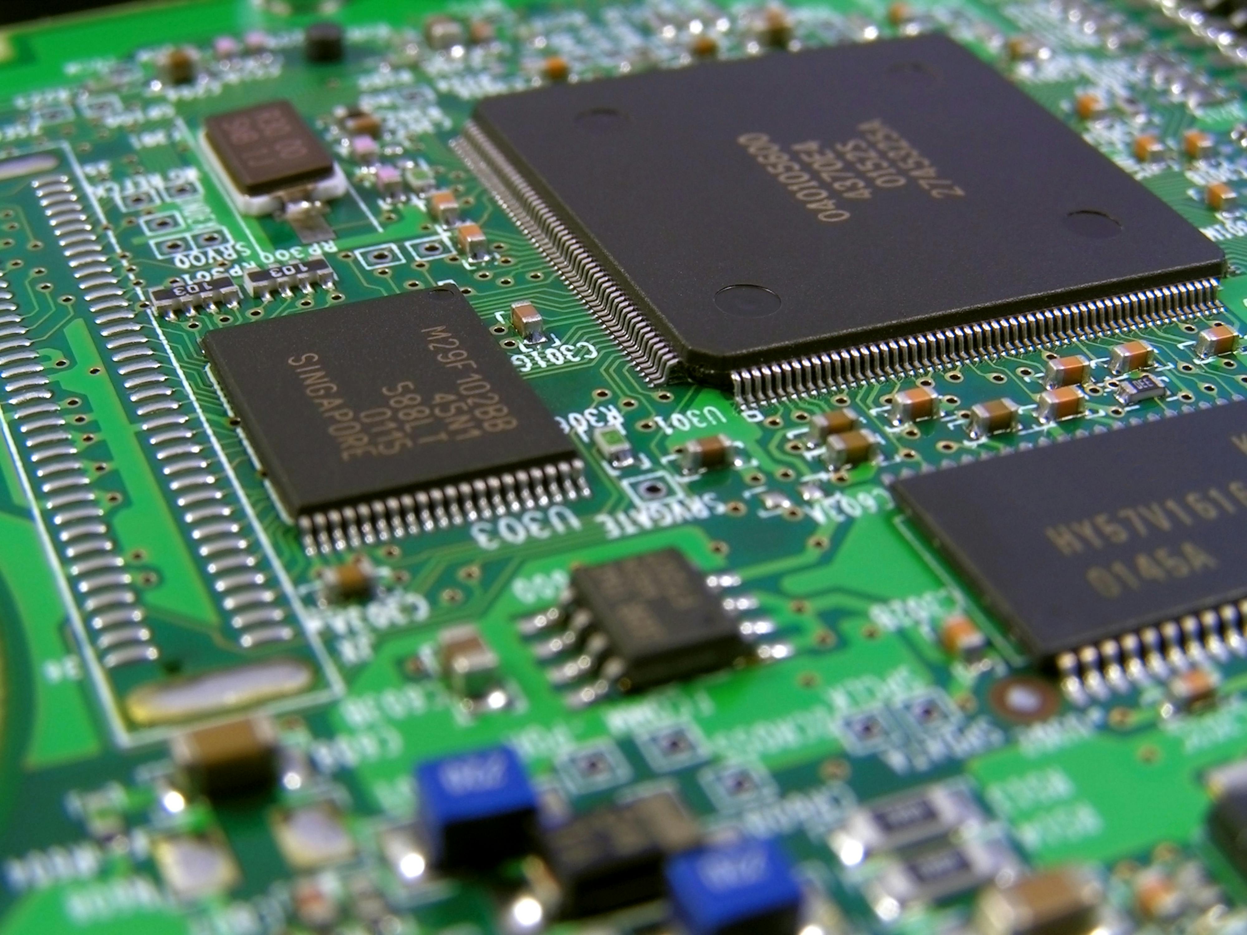
Atlas Core of Engineers, an industrial-controls firm, is collaborating with semiconductor companies to improve operational resiliency through advanced automation. By retrofitting existing facilities and establishing new ones, Atlas aims to minimize downtime in a sector where interruptions are intolerable. Ahmad Jodeh, the firm's owner, emphasizes the importance of PROFINET technology in overcoming the limitations of traditional PROFIBUS systems, particularly in terms of bandwidth and troubleshooting. The semiconductor industry is undergoing significant changes, driven by global competition and technological advancements. U.S. manufacturers are investing heavily in domestic chip production, spurred by incentives from the CHIPS and Science Act. This shift is prompting companies to enhance their automation capabilities to maintain competitiveness, with PROFINET playing a crucial role in achieving higher efficiency and reliability in operations. As semiconductor firms transition to PROFINET, they are leveraging its network redundancy features to ensure continuous operation. This capability allows for the establishment of multiple communication routes, which is vital in preventing downtime. The ongoing evolution in the semiconductor landscape highlights the need for innovative solutions that can adapt to rapid changes while ensuring operational integrity.
Factory / Digital Transformation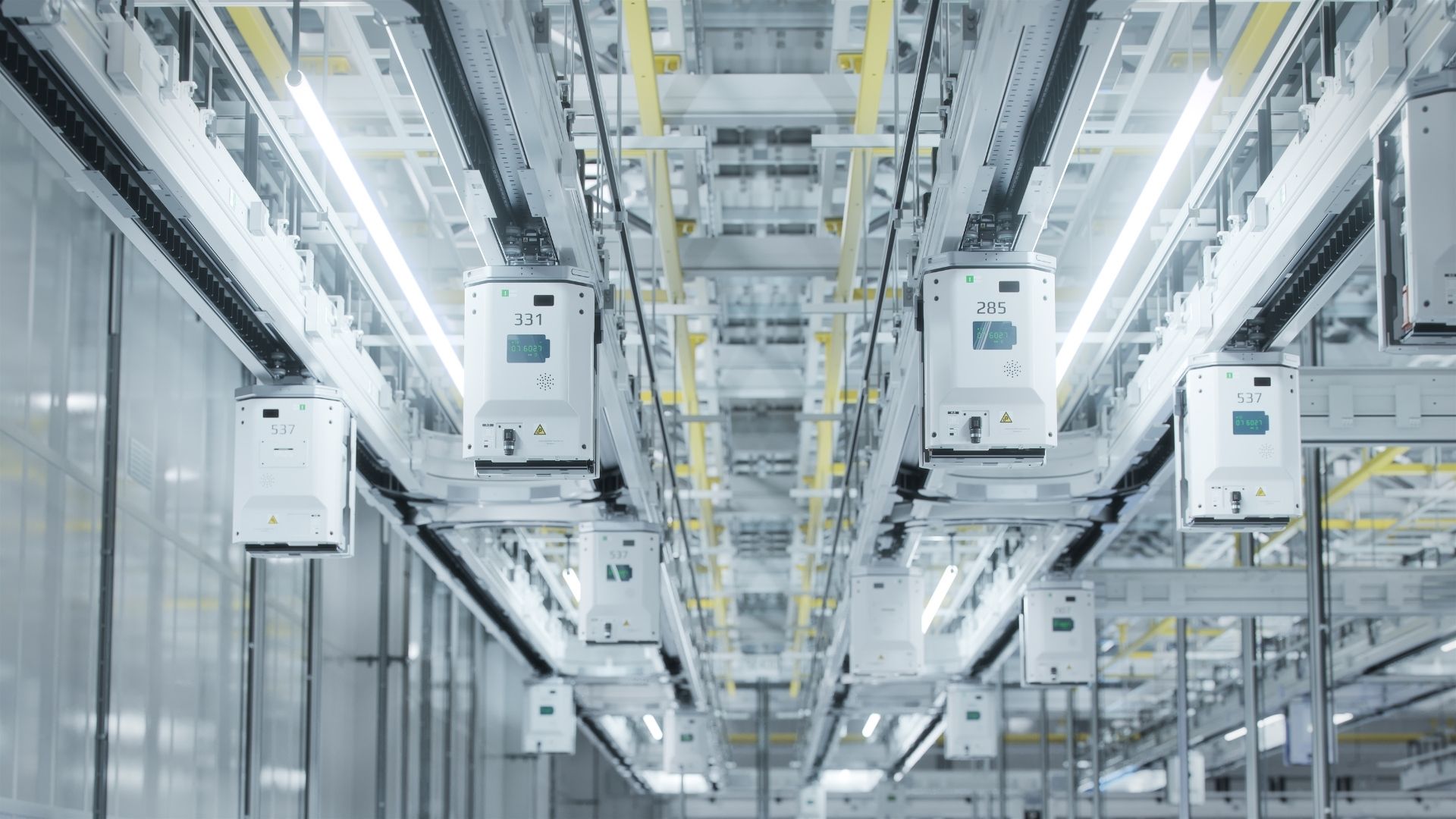
US semiconductor giant breaks ground on $9.3-billion memory chip plant expansion in Japan
Micron Technology has officially commenced the expansion of its manufacturing facility in Hiroshima Prefecture, Japan. This significant development took place on October 25, 2023, as the company aims to enhance its production capabilities in response to the growing global demand for semiconductor products. The expansion is part of Micron's broader strategy to invest in advanced manufacturing technologies and increase its output to support various industries reliant on memory and storage solutions. By bolstering its operations in Japan, Micron seeks to solidify its position in the competitive semiconductor market and contribute to the local economy through job creation and technological advancement. The project underscores the company's commitment to innovation and its role in addressing the challenges posed by supply chain disruptions in the semiconductor sector.
Innovation
ON Semiconductor: Mispriced 800V-1200V AI Power And Physical AI Shift
ON Semiconductor has received a "Buy" rating, indicating a favorable outlook for investors as the company is expected to experience significant growth by 2027-2028. This positive assessment follows ON's strategic acquisition of Synaptics for $7 billion and the development of its proprietary Treo platform, which is projected to expand its total addressable market to $243 billion by 2030. Key factors driving this growth include a tenfold increase in content for 800V AI data center racks and a targeted margin expansion to 53%. Additionally, the company aims to reduce its reliance on the global auto market by capitalizing on exports of electric vehicles from China. However, analysts caution that risks remain, particularly concerning the integration of Synaptics, potential delays in retrofitting data centers, fluctuations in the average selling price of silicon carbide in China, and the company's balance sheet leverage. For those looking to invest in ON Semiconductor, the FTXL ETF is suggested as a diversified option to gain exposure to the company's performance.
SYNA FTXL ON Esxeleryn Analytics
Critical Semiconductor Testing for AI and Data Center Power Demands
As artificial intelligence (AI) drives significant power requirements in data centers, the importance of thorough semiconductor testing has escalated. This trend highlights the growing challenges faced by data centers in managing energy consumption while ensuring optimal performance. The new video series aims to provide insights into these critical testing processes and their implications for the industry. The increasing reliance on AI technologies necessitates a robust approach to semiconductor testing, which is essential for maintaining efficiency and reliability in data centers. As power demands rise, organizations must adapt their testing methodologies to address these challenges effectively. This shift underscores the vital role that semiconductor testing plays in supporting the evolving landscape of AI and data center operations. Looking ahead, industry stakeholders should monitor advancements in semiconductor testing techniques and their impact on energy management in data centers. The ongoing development of testing protocols will be crucial in ensuring that data centers can meet the growing power demands associated with AI applications. No further timeline was disclosed at the time of publication.
"Building a Brain for Robots: How Chip Bridge Semiconductor Positions Itself in the Foundation of Embodied Intelligent Computing Power"
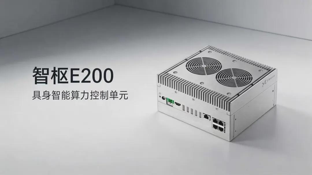
Chip Bridge Semiconductor is making significant strides in the development of advanced computing technology aimed at enhancing robotic intelligence. The company is focused on creating a new generation of chips designed to serve as the foundational brain for robots, enabling them to process information and respond to their environments more effectively. This initiative comes at a time when the demand for embodied intelligent computing is rapidly increasing, driven by advancements in artificial intelligence and automation. Located in Silicon Valley, Chip Bridge Semiconductor is leveraging cutting-edge research and development to innovate in this competitive field. The company aims to address the growing need for robots that can operate autonomously in various settings, from manufacturing to healthcare. By integrating sophisticated algorithms with powerful semiconductor technology, Chip Bridge is positioning itself as a leader in the robotics sector. The motivation behind this initiative is to create robots that not only perform tasks but also learn and adapt to new challenges, thereby improving efficiency and productivity across industries. Through strategic partnerships and investments in research, Chip Bridge Semiconductor is working to refine its chip designs and enhance their capabilities, ensuring that they meet the evolving needs of the market. As the landscape of robotics continues to evolve, Chip Bridge Semiconductor’s efforts could play a crucial role in shaping the future of intelligent machines, making them more capable and versatile in their applications.
Robotics Automation AI
ON Semiconductor strikes $7 billion deal for Synaptics in physical AI push
ON Semiconductor announced that a recent deal will increase its total addressable market by $30 billion, bringing the total to $243 billion by 2030. This strategic move reflects the company's commitment to expanding its footprint in the semiconductor industry, capitalizing on growing demand for advanced technologies. The announcement underscores ON Semiconductor's efforts to enhance its competitive position and drive future growth in an evolving market landscape.

Semiconductor Review: Enhancing Semiconductor Manufacturing Through Intelligent Automation
Teradyne has been acknowledged by Semiconductor Review as the leading provider of semiconductor test and robotic solutions, highlighting the company's significant advancements in the integration of artificial intelligence within the semiconductor industry. This recognition comes amid a growing trend where the boundaries between semiconductor testing and factory automation are increasingly merging. The award underscores Teradyne's commitment to innovation and excellence in developing technologies that enhance efficiency and precision in semiconductor manufacturing. As the industry evolves, the incorporation of AI is expected to play a crucial role in streamlining operations and improving overall productivity.

Stocks Rise With Nvidia Leading as Semiconductor Companies Surge
U.S. stocks experienced an upward trend on Thursday, driven by a continued surge in semiconductor shares following a strong performance the previous day. Nvidia Corp. emerged as the leading contributor to gains in the S&P 500 Index, significantly boosting investor sentiment. Additionally, the Philadelphia Semiconductor Index, commonly referred to as the SOX, soared over 6%, reaching a record high. This rally reflects growing optimism in the technology sector, particularly in semiconductor companies, as they benefit from increasing demand and advancements in technology.
NMS:NVDA
NVIDIA and TSMC Bring AI Into Fabs to Advance Semiconductor Design and Manufacturing
NVIDIA has revealed that TSMC, the leading semiconductor manufacturer globally, is leveraging NVIDIA's accelerated computing and artificial intelligence technologies to enhance its semiconductor design and manufacturing processes. This collaboration aims to improve efficiency and innovation in the semiconductor industry, reflecting the growing importance of advanced computing solutions in driving technological advancements. The announcement underscores the strategic partnership between the two companies, highlighting their commitment to pushing the boundaries of semiconductor capabilities.
SAIC and Semiconductor Firms Invest in Blue Dot Touch Control: A Strategic Move in Robotics
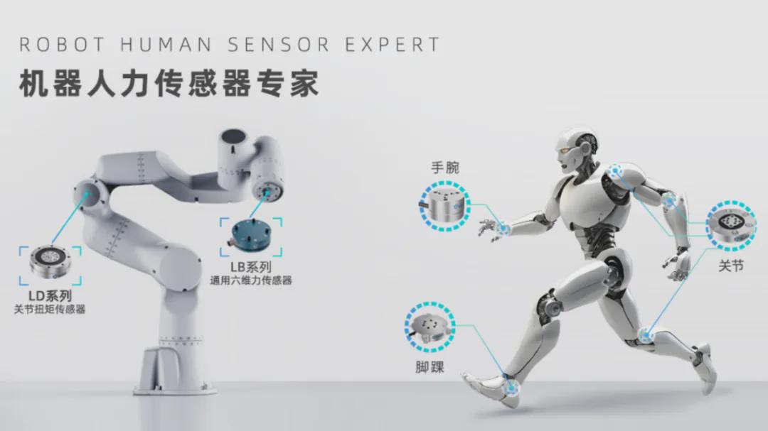
Blue Dot Touch Control has successfully obtained substantial funding from prominent industry leaders, including SAIC and various semiconductor companies. This investment underscores the increasing importance of force sensors in the field of robotics. As the need for accurate and nuanced interactions with the physical environment intensifies, these sensors are emerging as vital elements in the development of humanoid robots. This trend is not only fostering innovation but also intensifying competition within the robotics sector.
Force Sensors Humanoid Robots Robotics Technology Investment in Robotics AI and Robotics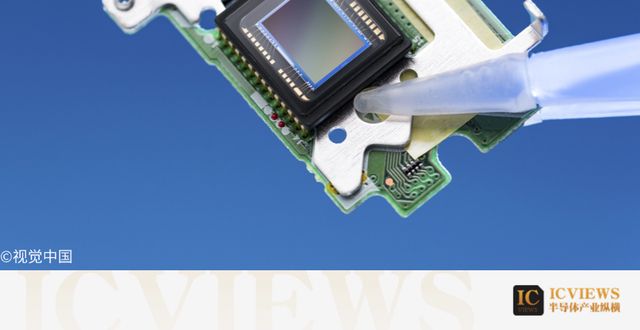
Geke Semiconductor's 50MP Image Sensors Cross 100 Million Shipments Milestone
Geke Semiconductor has announced a significant milestone, having shipped over 100 million units of its 50-megapixel image sensor products. This achievement highlights the growing demand for high-resolution sensors, which now represent a substantial portion of the company's revenue from mobile camera integrated circuits (CIS). The surge in shipments reflects the increasing reliance on advanced imaging technology in mobile devices, driven by consumer preferences for higher quality photography. As the market for mobile imaging continues to evolve, Geke Semiconductor's innovative sensor solutions are positioned to play a crucial role in meeting the needs of manufacturers and consumers alike.
Technology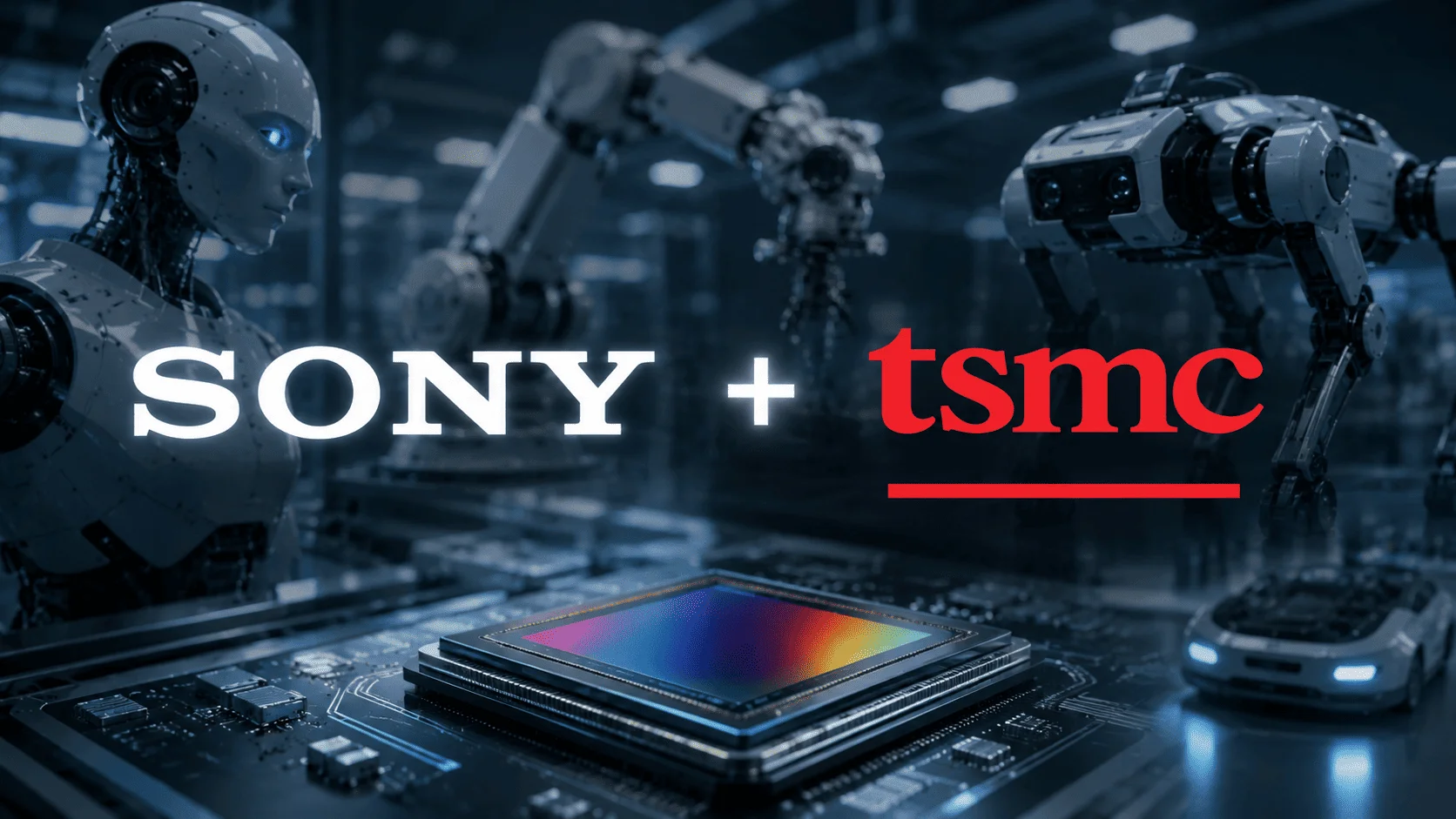
Sony Semiconductor Solutions and TSMC Plan Partnership to Develop Image Sensors for Physical AI
Sony Semiconductor Solutions and Taiwan Semiconductor Manufacturing Company (TSMC) have announced a strategic partnership aimed at developing and manufacturing next-generation image sensors. This collaboration, which was formalized through a non-binding memorandum of understanding, is set to explore future applications in sectors such as robotics, automotive systems, and physical AI. The partnership reflects both companies' commitment to advancing technology in these rapidly evolving fields.
AI AI Funding & Investment Robotics image sensors Japan Physical AI
NXP Semiconductors soars 26%, paces for its best day ever after earnings beat
Shares of the Dutch chipmaker experienced a remarkable surge of 26% on Wednesday, marking the largest increase since the company went public in 2010. This significant rise in stock value reflects growing investor confidence and optimism surrounding the company's future prospects in the semiconductor industry. The surge comes amid a broader recovery in technology stocks, as market sentiment improves following recent economic indicators. Investors are closely monitoring developments in the sector, particularly as demand for chips continues to rise globally. The company's strong performance is seen as a positive signal, suggesting robust growth potential in an increasingly competitive market.

Why Thermal Metrology Must Evolve for Next-Generation Semiconductors
A recent analysis highlights the challenges posed by rising power density, 3D integration, and innovative materials in the field of semiconductor thermal management. As the industry faces heat flux projections exceeding 1,000 W/cm² for next-generation accelerators, thermal management has emerged as the primary constraint on semiconductor scaling, shifting the focus from traditional lithography techniques. This shift is driven by advancements in heterogeneous integration and AI-driven power density. The study also addresses the implications of extreme material properties on thermal design, particularly in nanoscale thin films where conventional bulk assumptions are inadequate. It emphasizes the importance of engineered ultra-high-conductivity materials, such as diamond and boron arsenide, and the challenges of devices operating above 200 °C in wide-band gap systems. Furthermore, the analysis reveals that thermal boundary resistance at bonded interfaces and dielectric stacks has become a critical factor in ensuring reliability. To mitigate these issues, the report advocates for a thermal-first design workflow, which integrates measured, scale-appropriate thermal properties early in the design cycle. This approach aims to calibrate models, reduce uncertainty, and prevent costly failures in advanced packaging and 3D architectures. The findings underscore the urgent need for advanced metrology to keep pace with the evolving demands of semiconductor technology. A free whitepaper detailing these insights is available for download.
Semiconductors Thermal-management Scaling Type-whitepaper
Teradyne to Showcase Leading Semiconductor Test Solutions at IESA Vision Summit
Teradyne, Inc., a prominent provider of automated test equipment and advanced robotics, has announced significant developments in its product offerings. The company, based in North Reading, Massachusetts, revealed its latest innovations during a press conference held on October 10, 2023. This event showcased Teradyne's commitment to enhancing automation solutions, aimed at meeting the growing demands of various industries, including semiconductor manufacturing and electronics testing. The motivation behind these advancements is to address the increasing complexity of electronic devices and the need for more efficient testing processes. By integrating cutting-edge technology into their systems, Teradyne aims to improve accuracy and reduce time-to-market for its clients. The company highlighted how these innovations will not only streamline operations but also contribute to cost savings for manufacturers. During the presentation, Teradyne executives outlined the technical specifications and benefits of the new products, emphasizing their potential impact on the industry. The event attracted attention from industry leaders and stakeholders, underscoring Teradyne's position as a key player in the automation sector. As the demand for advanced robotics and testing equipment continues to rise, Teradyne's latest offerings are poised to play a crucial role in shaping the future of automated solutions.

Semiconductor Sourcing for Robotics: Managing Lead Times and Component Lifecycle Risks
As global adoption of robotics continues to surge, procurement and engineering teams are reassessing their strategies for managing lead times, component lifecycles, and sourcing risks. This shift is driven by the increasing volatility in semiconductor markets, which has heightened the challenges faced by these teams. The need for a more agile and responsive approach is becoming critical as companies strive to maintain efficiency and competitiveness in a rapidly evolving technological landscape. By adapting their processes, organizations aim to mitigate risks associated with supply chain disruptions and ensure a steady flow of essential components for their robotic systems.

Semiconductor Innovations for the Next Generation of Robots
Texas Instruments (TI) has unveiled a new technology aimed at enhancing the performance of motors by integrating FETs, drivers, and current sensing into a single compact package. This innovation addresses the growing demand for high power density and precise control in motor applications, particularly in industries where space is at a premium. By reducing the size of the circuit board, TI's solution not only optimizes performance but also simplifies the design process for engineers. The announcement comes as part of TI's ongoing commitment to advancing motor control technology, reflecting the company's response to industry needs for more efficient and space-saving solutions. This development is expected to significantly impact various sectors, including automotive and industrial automation, where compact and efficient motor systems are crucial.

Semiconductor Digest | 2026 Outlook: Executive Viewpoints
As the semiconductor industry approaches 2026, the influence of artificial intelligence (AI) is becoming increasingly prominent. Shannon Poulin, President of a leading technology firm, emphasized the critical role of testing in enabling AI advancements within semiconductor manufacturing. This shift is driven by the industry's need to enhance efficiency and innovation in production processes. By integrating AI into testing protocols, companies can streamline operations, reduce costs, and improve product quality. The ongoing evolution highlights the necessity for semiconductor manufacturers to adapt to AI technologies to remain competitive in a rapidly changing market landscape.

Texas Instruments Deploys UBTECH Humanoids in Strategic Semiconductor Push
Texas Instruments, a leading American semiconductor company, has announced a collaboration with UBTECH Robotics to integrate Walker S2 humanoid robots into its production lines. This partnership signifies UBTECH's strategic entry into the high-precision semiconductor industry. The deployment of these advanced robots aims to enhance operational efficiency and precision in manufacturing processes. The initiative reflects a growing trend in the tech sector, where automation and robotics are increasingly utilized to streamline production and improve output quality. The integration of Walker S2 units is expected to commence shortly, aligning with Texas Instruments' commitment to innovation and technological advancement in its manufacturing operations.
Business China UBTECH Robotics
Semiconductor Digest: Co-Packaged Optics: Test Challenges for Data Center Technology of the Future
AI-driven data centers are pushing the boundaries of speed and efficiency, prompting a growing demand for technologies that can provide higher bandwidth while consuming less power. In response to this need, researchers are increasingly turning to silicon photonics (SiPh), a technology that utilizes light to transmit data, significantly enhancing data transfer rates and reducing energy consumption. As data centers continue to expand and evolve, the integration of SiPh is seen as a crucial step towards achieving sustainable and high-performance computing solutions. This shift is expected to play a vital role in meeting the escalating demands of AI applications and cloud services, which require rapid data processing and transmission capabilities. The advancements in silicon photonics are anticipated to revolutionize the infrastructure of data centers, making them more efficient and environmentally friendly.

EE Times: Flexible Test Strategies Keeping Pace with Semiconductor Evolution
The semiconductor industry is undergoing a significant transformation, propelled by innovations in artificial intelligence, advanced packaging techniques, heterogeneous integration, and edge computing technologies. This evolution is reshaping semiconductor design and manufacturing processes, enabling companies to enhance performance and efficiency. As these advancements continue to emerge, industry leaders are adapting their strategies to meet the growing demands for more powerful and versatile chips. The shift is not only impacting production methods but also influencing the broader technology landscape, as semiconductors play a crucial role in powering a wide array of devices and applications. This ongoing change is expected to drive competition and collaboration among key players in the market, ultimately leading to new opportunities and challenges within the sector.
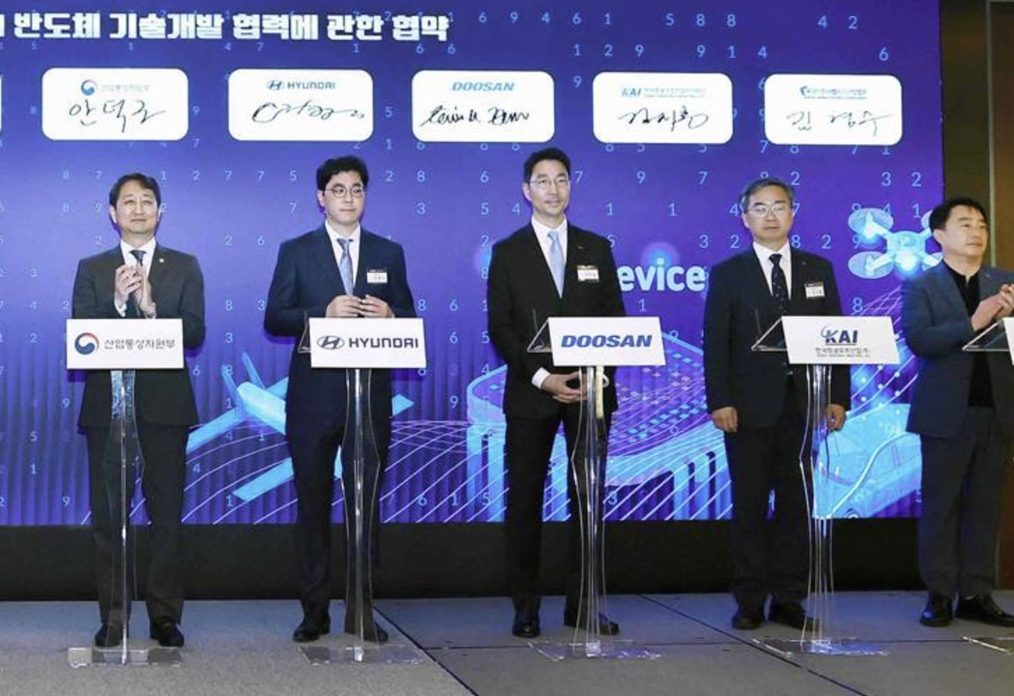
Doosan Robotics Signs MoU for 'K-On-Device AI Semiconductor Development Collaboration'
On May 20, Doosan Robotics announced a significant collaboration by signing a memorandum of understanding for the "K-On-Device AI Semiconductor Development Collaboration" during the AI Semiconductor Collaboration Forum at The Westin Chosun Hotel in Seoul. The event was attended by key stakeholders, including the Ministry of Trade, Industry and Energy, the Korea Evaluation Institute of Industrial Technology, and major companies such as LG Electronics and Hyundai Motor Company, alongside industry associations like the Korea Fabless Industry Association. This government-led initiative aims to establish a strong presence in the burgeoning Physical AI market, with planned projects valued at approximately KRW 1 trillion over the next five years. As the AI semiconductor landscape transitions from expensive, cloud-based systems to more efficient, on-device applications, the participating entities will engage in research and development to create AI semiconductors tailored for four key sectors: automotive, IoT and home appliances, machinery and robotics, and defense. Doosan Robotics, representing the machinery and robotics sector, has been involved in the project planning from the beginning and will collaborate closely with fabless companies throughout the entire development process. This includes joint development, validation of AI semiconductors and software, integration, and mass production, fostering a sustainable cycle of demand and supply while bolstering South Korea's AI semiconductor capabilities. A spokesperson from Doosan Robotics emphasized the increasing demand for power-efficient and intelligent AI semiconductors that can perform complex tasks in unpredictable environments, highlighting the company's commitment to enhancing its technological edge through this partnership.

Teradyne Announces Succession Plan for Semiconductor Test Division
Teradyne, Inc., a leading technology company based in North Reading, Massachusetts, has appointed Shannon Poulin as its new executive, succeeding Rick. This leadership change was announced today, reflecting the company's ongoing commitment to strengthening its management team. The decision to bring Poulin on board is part of Teradyne's strategy to enhance its operational capabilities and drive future growth in the competitive tech landscape.
Robotics needs a service framework.
RSF defines a common language for robot service capability, lifecycle operations, certification pathways, and service-provider networks.
Join the RobotToday community on LinkedIn
Daily robotics news, in-depth analysis, conference highlights, and discussions with professionals worldwide.